HNST WELCOME! 0755-23173910
English /中文
CATEGORY
View All
你当前的浏览器版本过低或不支持。请升级或更换浏览器。推荐浏览器 Chrome Edge。
The success of protecting the system from the impact of electrostatic discharge (ESD) largely depends on the design of printed circuit boards (PCBs). Although selecting the appropriate transient voltage suppressor (TVS) is the fundamental approach to ESD protection strategies, it is not within the scope of this article. The technical documentation on ti.com/esd provides many ESD selection guides that can guide you on how to choose the appropriate TVS diode type for a specific system. After selecting the appropriate TVS, using the strategies listed in this ESD Layout Guide to design PCB layouts will provide PCB designers with a successful way to protect the system from ESD impacts.


1. Introduction


TVS is a diode array (see Figure 1-2 for typical examples), which has a high impedance to the normal voltage present in the circuit. However, if the voltage exceeds the design range, the TVS diode will break down and divert the IESD to ground before it damages the protected system. Therefore, system designers need to reduce the impedance of IESD from the ESD source through TVS to ground.

The impedance provided to IESD is a function of the inherent impedance of TVS (in TVS diode arrays and packaging) and the PCB layout between the ESD source and TVS ground. TVS is typically designed to provide the lowest possible ground impedance for IESD within its overall design limitations. After selecting the appropriate TVS, reducing the impedance between the ESD source and TVS ground on the PCB layout is a critical stage in the design.


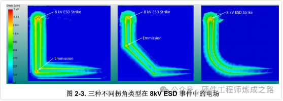
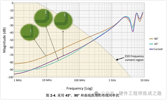
Another issue arising from the rapidly changing IESD is that its associated rapidly changing electromagnetic field (EM) can cause interference (EMI) to couple to other circuits on the PCB, especially in the area between the ESD source and TVS. Once the TVS diverts the IESD to ground, the wiring between the TVS and the protected IC should be relatively unaffected by EMI. Therefore, between the ESD source and TVS, unprotected circuits should not be adjacent to the wiring of the ESD protection circuit. In order to minimize EMI radiation, ideally, the circuit wiring between the ESD source and TVS should not have corners exceeding 45 degrees or curves with large radii.


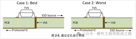
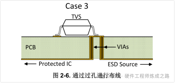
In today's PCB layout, board space is very valuable. IC, Including TVS, they must be designed very compactly. In addition, the placement density of ICs on PCBs is constantly increasing. Multilayer PCB circuit boards and wiring heavily rely on via holes to maximize density, thereby reducing system size and increasing system feature settings. This PCB architecture (especially related to layer switching and via) plays an important role in diverting IESD to ground through TVS. The use of via holes to wire circuits to TVS may result in significant VESD voltage differences on the protected IC. Usually, placing a via between the ESD source and TVS has adverse effects, but in some cases, designers may have to resort to this strategy. Even in the above situations, if handled properly, VESD can still be minimized on the protected IC as much as possible.
 
The grounding scheme is crucial for preventing ESD. Using chassis grounding for TVS (different from digital and/or analog grounding implemented by inductance) can effectively avoid ESD related failures. However, when wiring high-speed circuits on multiple grounding planes, this poses significant challenges. Therefore, many designs use a common ground for protected circuits. The grounding plane is essential for TVS to successfully consume IESD without increasing VESD. The electrical connection of the ground grounded chassis, such as the PCB grounding through-hole used for chassis screws, directly adjacent to the TVS grounding and ESD source grounding (such as the connector shielding layer), provides a reasonable method to keep the grounding offset at the protected IC to a minimum. If the system cannot utilize chassis ground grounding, tightly coupled multi-layer grounding planes can help keep ground drift at the protected IC to a minimum.
 
Summarizing these parameters, the factors that successfully protect the system from ESD impact include:
 
Control the impedance around TVS to consume ESD current IESD
 
Limit the impact of EMI on unprotected circuits
 
• Proper use of via to maximize ESD consumption by TVS

Figure 2-1 shows four parasitic inductors: L1 and L2 are the inductance in the circuit between the ESD source (usually a connector) and TVS, L3 is the inductance between TVS and ground, and L4 is the inductance between TVS and the protected IC.


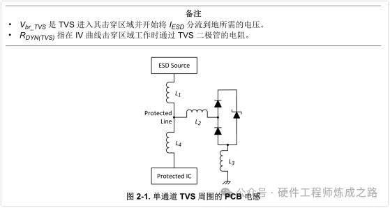
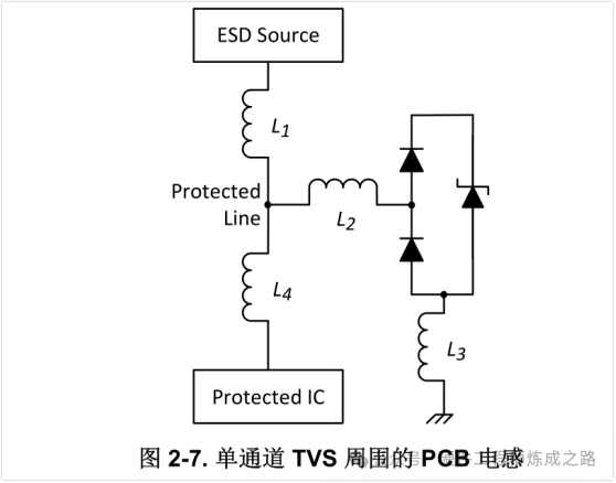
Without considering through holes, inductors L1 and L4 typically depend on design constraints, such as impedance controlled signal lines. However, by making L4 much larger than L1, IESD can still "turn" to TVS. This is achieved by placing the TVS near the ESD source and keeping the protected IC away from the TVS (such as near the middle of the PCB), as allowed by PCB design rules. This can effectively generate an effect of L4>>L1, helping to redirect IESD to TVS. Placing TVS close to the connector can also reduce EMI radiation into the system. In a well-designed system, the inductor at L2 should not exist. This indicates the presence of residual piles between TVS and the protected line. This design practice should be avoided. The protected circuit should be directly connected from the ESD source to the pins of TVS, ideally with no via on the path. The inductor at L3 represents the inductance between TVS and the ground terminal. The inductance value should be minimized as much as possible and may be the main parasitic effect affecting VESD.


The voltage provided to the "protected line" node will be VESD=Vbr-TVS+IESD RDYN (TVS)+(L2+L3) (dIESD/dt). Therefore, PCB designers need to minimize L3 and eliminate L2 as much as possible.
 
 
The method of minimizing L3 as much as possible is introduced in section 2.4. The method of minimizing L1 as much as possible is introduced in sections 2.2 and 2.3.
 
Summary
 
 
Minimize the inductance between the ESD source and the grounding path through TVS as much as possible
 
Place TVS near the connector, as allowed by design rules
 
Make the distance between the protected IC and TVS far exceed the distance from TVS to the connector
 
Do not use residual stakes between TVS and protected lines, wiring directly from ESD source to TVS

Another aspect of PCB layout is to consider the style of the corners between the ESD source and TVS. Corners often emit EMI during IESD. The best wiring method from ESD source to TVS is to use the shortest possible straight path. In addition to reducing the impedance in the IESD grounding path, shortening the length of this path can also reduce the EMI radiated inside the system. If a corner is required, the wiring should be bent at the maximum radius. If PCB technology does not allow for bent wiring, a 45 ° corner is the maximum angle.

In Figures 2-3, note that for a 90 ° corner, it is a significant source of EMI. The electric field at the corner is at least 7kV. This will cause any radius less than 2.6mm (in air) to generate an arc (ionization). The EMI of the 45 ° curve is not as significant. To further demonstrate the influence of corner styles, Figure 2-4 illustrates the crosstalk generated between parallel wiring using these three corner types. The coupling at the 90 ° corner is higher than at other corners, especially in the ESD frequency component region.

Summary
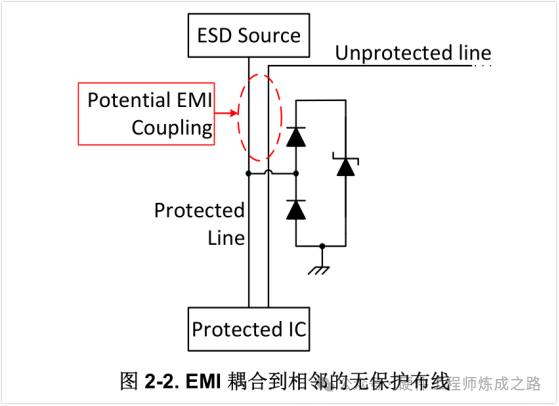
Do not place unprotected circuits in the area between the ESD source and TVS.
Place TVS near the connector, as allowed by design rules.
If possible, use straight wiring between the ESD source and TVS.
If corners must be used, curves should be preferred, and the maximum acceptable angle is 45 °.


2.3. Wiring through through-holes

In some cases, designers have no choice but to place TVS on a different layer than the ESD source. Figure 2-6 shows the third scenario, which is a variant of the second scenario. In the third scenario, IESD will be forced to enter the protection pin of TVS before establishing a path with the protected IC. This is an acceptable compromise for the second scenario.

These three situations represent examples of using via between the ESD source and the protected IC. It is best to avoid using this approach, but if necessary, the first scenario is the preferred method, and the second scenario should be avoided. If there is no alternative method, the third scenario is acceptable.
 
 
Summary
• If possible, avoid via between ESD source and TVS
 
If a via is required between the ESD source and the protected IC, please wire directly from the ESD source to TVS before using the via
 
Only when TVS has a grounding path with extremely low inductance, successfully eliminating all parasitic inductance between ESD source and TVS will be effective. The TVS grounding pin should be connected to the grounding plane of the same layer, and this grounding plane should be coupled with another grounding plane directly adjacent to the layer. These grounding planes should be spliced together through vias, with one of the vias adjacent to the grounding pin of the TVS (see Figure 2-8).
 
Figure 2-7 shows the PCB inductance around a single channel TVS (as shown in Figure 2-1 earlier). This section only considers the inductance at L3. Please note that, with the elimination of L2, the voltage provided to the protected IC during ESD events will be VESD=Vbr-TVS+IESD RDYN (TVS)+L3 (dIESD/dt), while at 8kV, dIESD/dt=4 x 10 ^ 10. Obviously, L3 must be minimized as much as possible.

To reduce L3, it is best to directly connect the TVS ground pin to the coupled ground plane. Figure 2-8 shows the grounding pad of the TVS connected to the top grounding plane. There are four splicing through holes here to connect the top grounding plane to the internal grounding plane. Depending on the number of layers and circuit board design, these via holes may be connected to multiple ground plane layers. The bolt position of the grounding chassis is also very close to the TVS grounding pad. A grounding scheme similar to this will bring an extremely low grounding impedance to L3.

Due to the encapsulation type, Figures 2-8 are independent of certain types of TVS. TVS packaged in BGA with ground pins surrounded by other pins need to be connected to an internal ground plane through a via, preferably multiple coupled ground planes. Figure 2-9 shows a TVS with this grounding pin.

A via needs to be constructed to provide the smallest possible impedance. Due to the skin effect, maximizing the surface area of GND via can minimize the impedance of the grounding path. Therefore, the diameter of the through-hole pad and the diameter of the through-hole drill should be maximized to maximize the surface area of the outer and inner surfaces of the through-hole. The grounding plane should not be disconnected in the vicinity of the GND through-hole. If possible, connect the GND via to the grounding plane on multiple layers to minimize impedance. GND vias should be filled with non-conductive fillers (such as resin) instead of conductive fillers, in order to retain the surface area inside the vias generated by drilling. GND vias should be electroplated on SMD pads. The gap between GND vias and non grounded planes (such as power planes) should be kept to a minimum. This will increase capacitance, which can reduce impedance.
3. Conclusion


Summary:
 
 
Control the impedance around TVS to dissipate ESD current IESD:
- Minimize the inductance between the ESD source and the grounding path through TVS as much as possible
- Place TVS near the connector, as allowed by design rules
Make the distance between the protected IC and TVS far exceed the distance from TVS to the connector.
- Do not use residual stakes between TVS and protected lines, wiring directly from ESD source to TVS
 
It is crucial to minimize the inductance between TVS and ground as much as possible
 
• Limit the impact of EMI on unprotected circuits:
- Do not place unprotected circuits in the area between the ESD source and TVS
- Place TVS near the connector, as allowed by design rules
 
- If possible, use straight wiring between ESD source and TVS
- If corners must be used, curves should be preferred, and the maximum acceptable angle is 45 °
 
 
• Use through-holes correctly to maximize ESD dissipation through TVS as much as possible:
- If possible, avoid using via between ESD source and TVS
If a via is required between the ESD source and the protected IC, please wire directly from the ESD source to TVS before using the via
 
• Use a grounding scheme with extremely low impedance:
 

Product Recommendation

Recommend Article